 |
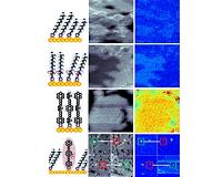
Berkeley CA (SPX) Nov 18, 2010 Sunlight represents the cleanest, greenest and far and away most abundant of all energy sources, and yet its potential remains woefully under-utilized. High costs have been a major deterrant to the large-scale applications of silicon-based solar cells. Nanopillars - densely packed nanoscale arrays of optically active semiconductors - have shown potential for providing a next generation of relatively cheap and scalable solar cells, but have been hampered by efficiency issues. The nanopillar story, however, has taken a new twist and the future for these materials now looks brighter than ever. "By tuning the shape and geometry of highly ordered nanopillar arrays of germanium or cadmium sulfide, we have been able to drastically enhance the optical absorption properties of our nanopillars," says Ali Javey, a chemist who holds joint appointments with the Lawrence Berkeley National Laboratory (Berkeley Lab) and the University of California (UC) at Berkeley. Javey, a faculty scientist with Berkeley Lab's Materials Sciences Division and a UC Berkeley professor of electrical engineering and computer science, has been at the forefront of nanopillar research. He and his group were the first to demonstrate a technique by which cadmium sulfide nanopillars can be mass-produced in large-scale flexible modules. In this latest work, they were able to produce nanopillars that absorb light as well or even better than commercial thin-film solar cells, using far less semiconductor material and without the need for anti-reflective coating. "To enhance the broad-band optical absorption efficiency of our nanopillars we used a novel dual-diameter structure that features a small (60 nanometers) diameter tip with minimal reflectance to allow more light in, and a large (130 nanometers) diameter base for maximal absorbtion to enable more light to be converted into electricity," Javey says. "This dual-diameter structure absorbed 99-percent of incident visible light, compared to the 85 percent absorbtion by our earlier nanopillars, which had the same diameter along their entire length." Theoretical and experimental works have shown that 3-D arrays of semiconductor nanopillars - with well-defined diameter, length and pitch - excel at trapping light while using less than half the semiconductor material required for thin-film solar cells made of compound semiconductors, such as cadmium telluride, and about one-percent of the material used in solar cells made from bulk silicon. But until the work of Javey and his research group, fabricating such nanopillars was a complex and cumbersome procedure. Javey and his colleagues fashioned their dual diameter nanopillars from molds they made in 2.5 millimeter-thick alumina foil. A two-step anodization process was used to create an array of one micrometer deep pores in the mold with dual diameters - narrow at the top and broad at the bottom. Gold particles were then deposited into the pores to catalyze the growth of the semiconductor nanopillars. "This process enables fine control over geometry and shape of the single-crystalline nanopillar arrays, without the use of complex epitaxial and/or lithographic processes," Javey says. "At a height of only two microns, our nanopillar arrays were able to absorb 99-percent of all photons ranging in wavelengths between 300 to 900 nanometers, without having to rely on any anti-reflective coatings." The germanium nanopillars can be tuned to absorb infrared photons for highly sensitive detectors, and the cadmium sulfide/telluride nanopillars are ideal for solar cells. The fabrication technique is so highly generic, Javey says, it could be used with numerous other semiconductor materials as well for specific applications. Recently, he and his group demonstrated that the cross-sectional portion of the nanopillar arrays can also be tuned to assume specific shapes - square, rectangle or circle - simply by changing the shape of the template. "This presents yet another degree of control in the optical absorption properties of nanopillars," Javey says. Javey's dual-diameter nanopillar research was partially funded through the National Science Foundation's Center of Integrated Nanomechanical Systems (COINS) and through Berkeley Lab LDRD funds. A paper describing this research appears on-line in the journal NANO Letters under the title "Ordered Arrays of Dual-Diameter Nanopillars for Maximized Optical Absorption." Co-authoring the paper with Javey were Zhiyong Fan, Rehan Kapadia, Paul Leu,Xiaobo Zhang, Yu-Lun Chueh, Kuniharu Takei, Kyoungsik Yu, Arash Jamshidi, Asghar Rathore, Daniel Ruebusch and Ming Wu.
Share This Article With Planet Earth
Related Links Ali Javey Lab Nano Technology News From SpaceMart.com Computer Chip Architecture, Technology and Manufacture
 Nanoscale Probe Reveals Interactions Between Surfaces And Single Molecules
Los Angeles CA (SPX) Nov 18, 2010 As electronics become smaller and smaller the need to understand nanoscale phenomena becomes greater and greater. Because materials exhibit different properties at the nanoscale than they do at larger scales, new techniques are required to understand and to exploit these new phenomena. A team of researchers led by Paul Weiss, UCLA's Fred Kavli Chair in NanoSystems Sciences, has developed a ... read more |
|
| The content herein, unless otherwise known to be public domain, are Copyright 1995-2010 - SpaceDaily. AFP and UPI Wire Stories are copyright Agence France-Presse and United Press International. ESA Portal Reports are copyright European Space Agency. All NASA sourced material is public domain. Additional copyrights may apply in whole or part to other bona fide parties. Advertising does not imply endorsement,agreement or approval of any opinions, statements or information provided by SpaceDaily on any Web page published or hosted by SpaceDaily. Privacy Statement |


 del.icio.us
 Digg
Digg Reddit
 YahooMyWeb
 Google