| . |  |
. |
|
|
. |
by Staff Writers Washington DC (SPX) Jul 04, 2011
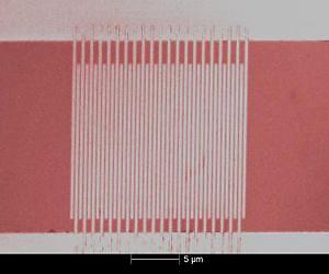
By swapping one superconducting material for another, researchers at the National Institute of Standards and Technology (NIST) have found a practical way to boost the efficiency of the world's fastest single-photon detector, while also extending light sensitivity to longer wavelengths. The new tungsten-silicon alloy could make the ultrafast detectors more practical for use in quantum communications and computing systems, experiments testing the nature of reality, and emerging applications such as remote sensing. The detector, made of superconducting nanowires, is one of several sensor designs developed or used at NIST to register individual photons (particles of light). The original nanowire detector, invented in Russia, uses wires made of niobium nitride and has a detection or quantum efficiency-ability to generate an electrical signal for each arriving photon-of less than 10 percent in its simplest, most compact model. NIST's tungsten-silicon alloy version has an efficiency of 19 to 40 percent over a broad wavelength range of 1280 to 1650 nanometers, including bands used in telecommunications.* The limitations are due mainly to imperfect photon absorption, suggesting that, with further design improvements, detector efficiency could approach 100 percent reliably, researchers say. Superconducting nanowire detectors have many advantages. They are very fast, able to count nearly a billion photons per second, and they operate over a large range of wavelengths, have low dark (false) counts, and produce strong signals, especially at telecom wavelengths. The detectors produce a signal when a photon breaks apart some of the electron pairs that carry current in the superconducting state, where the material has zero resistance. If the nanowires are narrow enough and the DC current across the device is very close to the transition between ordinary and super conductance, a resistive band temporarily forms across each wire, resulting in a measurable voltage pulse. Niobium nitride is difficult to make into nanowires that are narrow, long, and sensitive enough to work well. NIST researchers selected the tungsten-silicon alloy mainly because it has higher energy sensitivity, resulting in more reliable signals. A photon breaks more electron pairs in the tungsten-silicon alloy than in niobium nitride. The tungsten alloy also has a more uniform and less granular internal structure, making the nanowires more reliably sensitive throughout. As a result of the higher energy sensitivity, tungsten-silicon nanowires can have larger dimensions (150 nanometers wide versus 100 nanometers or less for niobium nitride), which enlarges the detectors' functional areas to more easily capture all photons. The NIST team now hopes to raise the efficiency of tungsten alloy detectors by embedding them in optical cavities, which trap light for extremely high absorption. High efficiency may enable the use of nanowire detectors in demanding applications such as linear optical quantum computing, which encodes information in single photons. An equally intriguing application may be an experiment to test quantum mechanics-the so-called "loophole-free Bell test." This test of what Einstein called "spooky action at a distance" depends critically on having a nearly 100-percent efficient photon detector. Tungsten-silicon detectors also are sensitive to longer wavelengths of light, in the mid-infrared range, which could be useful for applications such as laser-based remote sensing of trace gases. B. Baek, A.E. Lita, V. Verma and S.W. Nam. Superconducting a-WxSi1-x nanowire single-photon detector with saturated internal quantum efficiency from visible to 1850 nm. Applied Physics Letters 98, 251105. Published online June 21, 2011.
|
. |
|
| The content herein, unless otherwise known to be public domain, are Copyright 1995-2011 - Space Media Network. AFP and UPI Wire Stories are copyright Agence France-Presse and United Press International. ESA Portal Reports are copyright European Space Agency. All NASA sourced material is public domain. Additional copyrights may apply in whole or part to other bona fide parties. Advertising does not imply endorsement,agreement or approval of any opinions, statements or information provided by Space Media Network on any Web page published or hosted by Space Media Network. Privacy Statement |
 del.icio.us
 Digg
Digg Reddit
 Google