 |
West Lafayette, IN (SPX) May 26, 2011 Researchers have developed a method for creating single-crystal arrays of a material called graphene, an advance that opens up the possibility of a replacement for silicon in high-performance computers and electronics. Graphene is a one-atom-thick layer of carbon that conducts electricity with little resistance or heat generation. The arrays could make possible a new class of high-speed transistors and integrated circuits that consume less energy than conventional silicon electronics. The new findings represent an advance toward perfecting a method for manufacturing large quantities of single crystals of the material, similar to the production of silicon wafers. "Graphene isn't there yet, in terms of high quality mass production like silicon, but this is a very important step in that direction," said Yong P. Chen, corresponding author for the new study and Miller Family Assistant Professor of Nanoscience and Physics at Purdue University. Other researchers have grown single crystals of graphene, but no others have demonstrated how to create ordered arrays, or patterns that could be used to fabricate commercial electronic devices and integrated circuits. The hexagonal single crystals are initiated from graphite "seeds" and then grown on top of a copper foil inside a chamber containing methane gas using a process called chemical vapor deposition. The seeded growth method, critical to the new findings, was invented by Qingkai Yu, co-corresponding author for the study and an assistant professor at Texas State University's Ingram School of Engineering. "Using these seeds, we can grow an ordered array of thousands or millions of single crystals of graphene," said Yu, who pioneered the method while a researcher at the University of Houston. "We hope that industry will look at these findings and consider the ordered arrays as a possible means of fabricating electronic devices." Findings are detailed in a research paper appearing online this week and in the June issue of Nature Materials. The work was conducted by researchers at Purdue, the University of Houston, Texas State University, Brookhaven National Laboratory, Argonne National Laboratories and Carl Zeiss SMT Inc. Graphene currently is created in "polycrystalline" sheets made up of randomly positioned and irregularly shaped "grains" merged together. Having an ordered array means the positions of each crystal are predictable, and not random as they are in polycrystalline film. The arrays enable researchers to precisely position electronic devices in each grain, which is a single crystal having a seamless lattice structure that improves electrical properties, said Eric Stach, a researcher at Brookhaven and former Purdue professor of materials engineering. The new research findings confirmed a theory that the flow of electrons is hindered at the point where one grain meets another. The arrays of single-crystal grains could eliminate that problem. The researchers demonstrated that they could control the growth of the ordered arrays; were the first to demonstrate the electronic properties of individual grain boundaries; and they found that the edges of a single hexagonal crystal grain are parallel to well-defined directions in graphene's atomic lattice, revealing the orientation of each crystal. Knowing the orientation is necessary to measure the precise properties of the crystals, providing information needed to create better electronic devices. To determine the orientation of the graphene lattice, the researchers used two kinds of advanced microscopy techniques known as transmission electron microscopy and scanning tunneling microscopy. The techniques provided extremely high-resolution images of individual carbon atoms making up graphene. The electronic properties across the grain boundaries were measured using tiny electrodes connected to two adjoining grains. Findings demonstrated a higher electrical resistance at the grain boundaries and also showed that the boundaries hinder electrical conduction due to scattering of electrons. That finding was correlated using another technique called Raman spectroscopy.
The paper was authored by Yu and Purdue graduate student Luis A. Jauregui, Houston graduate student Wei Wu, Purdue graduate student Robert Colby, Purdue postdoctoral researcher Jifa Tian, along with 12 other researchers including Stach and Chen.
Yu, Wu, Houston graduate student Zhihua Su and colleagues created graphene single crystals, including the ordered arrays for the research at the University of Houston. Chen, Jauregui, Tian and colleagues studied these hexagonal graphene crystals, their edges and the grain boundaries using Raman spectroscopy, scanning tunneling microscopy and electrical measurements.
They have used various facilities in their Quantum Matter and Device Laboratory, Purdue's Birck Nanotechnology Center, as well as those in the National High Magnetic Field Laboratory and the Center for Nanoscale Materials at the Argonne National Laboratory. Stach and Colby documented the crystal orientation using transmission electron microscopes at Purdue's Birck Nanotechnology Center and at the Center for Functional Nanomaterials at the Brookhaven National Laboratory.
Share This Article With Planet Earth
Related Links Physics at Purdue University Computer Chip Architecture, Technology and Manufacture Nano Technology News From SpaceMart.com
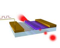 Graphene optical modulators could lead to ultrafast communications
Berkeley CA (SPX) May 11, 2011 Scientists at the University of California, Berkeley, have demonstrated a new technology for graphene that could break the current speed limits in digital communications. The team of researchers, led by UC Berkeley engineering professor Xiang Zhang, built a tiny optical device that uses graphene, a one-atom-thick layer of crystallized carbon, to switch light on and off. This switching abil ... read more |
|
| The content herein, unless otherwise known to be public domain, are Copyright 1995-2010 - SpaceDaily. AFP and UPI Wire Stories are copyright Agence France-Presse and United Press International. ESA Portal Reports are copyright European Space Agency. All NASA sourced material is public domain. Additional copyrights may apply in whole or part to other bona fide parties. Advertising does not imply endorsement,agreement or approval of any opinions, statements or information provided by SpaceDaily on any Web page published or hosted by SpaceDaily. Privacy Statement |


 del.icio.us
 Digg
Digg Reddit
 YahooMyWeb
 Google