 |
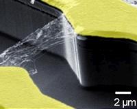
Boston MA (SPX) Mar 09, 2011 Graphene - a sheet of carbon atoms linked in a hexagonal, chicken wire structure - holds great promise for microelectronics. Only one atom thick and highly conductive, graphene may one day replace conventional silicon microchips, making devices smaller, faster and more energy-efficient. In addition to potential applications in integrated circuits, solar cells, miniaturized bio devices and gas molecule sensors, the material has attracted the attention of physicists for its unique properties in conducting electricity on an atomic level. Otherwise known as pencil "lead," graphene has very little resistance and allows electrons to behave as massless particles like photons, or light particles, while traveling through the hexagonal grid at very high speeds. The study of the physical properties and potential applications of graphene, however, has suffered from a lack of suitable carrier materials that can support a flat graphene layer while not interfering with its electrical properties. Researchers in the University of Arizona's physics department along with collaborators from the Massachusetts Institute of Technology and the National Materials Science Institute in Japan have now taken an important step forward toward overcoming those obstacles. They found that by placing the graphene layer on a material almost identical in structure, instead of the commonly used silicon oxide found in microchips, they could significantly improve its electronic properties. Substituting silicon wafers with boron nitride, a graphene-like structure consisting of boron and nitrogen atoms in place of the carbon atoms, the group was the first to measure the topography and electrical properties of the resulting smooth graphene layer with atomic resolution. The results are published in the advance online publication of Nature Materials. "Structurally, boron nitride is basically the same as graphene, but electronically, it's completely different," said Brian LeRoy, an assistant professor of physics and senior author of the study. "Graphene is a conductor, boron nitride is an insulator." "We want our graphene to sit on something insulating, because we are interested in studying the properties of the graphene alone. For example, if you want to measure its resistance, and you put it on metal, you're just going to measure the resistance of the metal because it's going to conduct better than the graphene." Unlike silicon, which is traditionally used in electronics applications, graphene is a single sheet of atoms, making it a promising candidate in the quest for ever smaller electronic devices. Think going from a paperback to a credit card. "It's as small as you can shrink it down," LeRoy said. "It's a single layer, you'll never get half a layer or something like that. You could say graphene is the ultimate in making it small, yet it 's still a good conductor." Stacked upon each other, 3 million sheets of graphene would amount to only 1 millimeter. The thinnest material on Earth, graphene brought the 2010 Nobel Prize to Andre Geim and Konstantin Novoselov, who were able to demonstrate its exceptional properties with relation to quantum physics. "Using a scanning tunneling microscope, we can look at atoms and study them," he added. "When we put graphene on silicon oxide and look at the atoms, we see bumps that are about a nanometer in height." While a nanometer - a billionth of a meter - may not sound like much, to an electron whizzing along in a grid of atoms, it's quite a bump in the road. "It's basically like a piece of paper that has little crinkles in it," LeRoy explains. "But if you put the paper, in this case the graphene, on boron nitride, it's much flatter. It smooths out the bumps by an order of magnitude." LeRoy admits the second effect achieved by his research team is a bit harder to explain. "When you have graphene sitting on silicon oxide, there are trapped electric charges inside the silicon oxide in some places, and these induce some charge in the overlying graphene. You get quite a bit of variation in the density of electrons. If graphene sits on boron nitride, the variation is two orders of magnitude less." In his lab, LeRoy demonstrates the first - and surprisingly low-tech - step in characterizing the graphene samples: He places a tiny flake of graphite - the stuff that makes up pencil "lead" - on sticky tape, folds it back on itself and peels it apart again, in a process reminiscent of a Rorschach Test. "You fold this in half," he explained, "and again, and again, until it gets thin. Graphene wants to peel off into these layers, because the bonds between the atoms in the horizontal layer are strong, but weak between atoms belonging to different layers. When you put this under an optical microscope, there will be regions with one, two, three, four or more layers. Then you just search for single-layer ones using the microscope." "It's hard to find the sample because it's very, very small," said Jiamin Xue, a doctoral student in LeRoy's lab and the paper's leading author. "Once we find it, we put it between two gold electrodes so we can measure the conductance." To measure the topography of the graphene surface, the team uses a scanning tunneling microscope, which has an ultrafine tip that can be moved around. "We move the tip very close to the graphene, until electrons start tunneling to it," Xue explained. "That's how we can see the surface. If there is a bump, the tip moves up a bit." For the spectroscopic measurement, Xue holds the tip at a fixed distance above the sample. He then changes the voltage and measures how much current flows as a function of that voltage and any given point across the sample. This allows him to map out different energy levels across the sample. "You want as thin an insulator as possible," LeRoy added. "The initial idea was to pick something flat but insulating. Because boron nitride essentially has the same structure as graphene, you can peel it into layers in the same way. Therefore, we use a metal as a base, put a thin layer of boron nitride on it and then graphene on top."
Share This Article With Planet Earth
Related Links University of Arizona Nano Technology News From SpaceMart.com Computer Chip Architecture, Technology and Manufacture
 Ultra Fast Photodetectors Out Of Carbon Nanotubes
Munich, Germany (SPX) Mar 08, 2011 Carbon nanotubes have a multitude of unusual properties which make them promising candidates for optoelectronic components. However, so far it has proven extremely difficult to analyze or influence their optic and electronic properties. A team of researchers headed by Professor Alexander Holleitner, a physicist at the Technische Universitaet Muenchen and member of the Cluster of Excellence ... read more |
|
| The content herein, unless otherwise known to be public domain, are Copyright 1995-2010 - SpaceDaily. AFP and UPI Wire Stories are copyright Agence France-Presse and United Press International. ESA Portal Reports are copyright European Space Agency. All NASA sourced material is public domain. Additional copyrights may apply in whole or part to other bona fide parties. Advertising does not imply endorsement,agreement or approval of any opinions, statements or information provided by SpaceDaily on any Web page published or hosted by SpaceDaily. Privacy Statement |


 del.icio.us
 Digg
Digg Reddit
 YahooMyWeb
 Google