 |
Atlanta GA (SPX) Mar 28, 2011 A new "templated growth" technique for fabricating nanoribbons of epitaxial graphene has produced structures just 15 to 40 nanometers wide that conduct current with almost no resistance. These structures could address the challenge of connecting graphene devices made with conventional architectures - and set the stage for a new generation of devices that take advantage of the quantum properties of electrons. "We can now make very narrow, conductive nanoribbons that have quantum ballistic properties," said Walt de Heer, a professor in the School of Physics at the Georgia Institute of Technology. "These narrow ribbons become almost like a perfect metal. Electrons can move through them without scattering, just like they do in carbon nanotubes." De Heer was scheduled to discuss recent results of this graphene growth process March 21st at the American Physical Society's March 2011 Meeting in Dallas. The research was sponsored by the National Science Foundation-supported Materials Research Science and Engineering Center (MRSEC). First reported Oct. 3 in the advance online edition of the journal Nature Nanotechnology, the new fabrication technique allows production of epitaxial graphene structures with smooth edges. Earlier fabrication techniques that used electron beams to cut graphene sheets produced nanoribbon structures with rough edges that scattered electrons, causing interference. The resulting nanoribbons had properties more like insulators than conductors. "In our templated growth approach, we have essentially eliminated the edges that take away from the desirable properties of graphene," de Heer explained. "The edges of the epitaxial graphene merge into the silicon carbide, producing properties that are really quite interesting." The "templated growth" technique begins with etching patterns into the silicon carbide surfaces on which epitaxial graphene is grown. The patterns serve as templates directing the growth of graphene structures, allowing the formation of nanoribbons and other structures of specific widths and shapes without the use of cutting techniques that produce the rough edges. In creating these graphene nanostructures, de Heer and his research team first use conventional microelectronics techniques to etch tiny "steps" - or contours - into a silicon carbide wafer whose surface has been made extremely flat. They then heat the contoured wafer to approximately 1,500 degrees Celsius, which initiates melting that polishes any rough edges left by the etching process. Established techniques are then used for growing graphene from silicon carbide by driving off the silicon atoms from the surface. Instead of producing a consistent layer of graphene across the entire surface of the wafer, however, the researchers limit the heating time so that graphene grows only on portions of the contours. The width of the resulting nanoribbons is proportional to the depth of the contours, providing a mechanism for precisely controlling the nanoribbon structures. To form complex structures, multiple etching steps can be carried out to create complex templates. "This technique allows us to avoid the complicated e-beam lithography steps that people have been using to create structures in epitaxial graphene," de Heer noted. "We are seeing very good properties that show these structures can be used for real electronic applications." Since publication of the Nature Nanotechnology paper, de Heer's team has been refining its technique. "We have taken this to an extreme - the cleanest and narrowest ribbons we can make," he said. "We expect to be able to do everything we need with the size ribbons that we are able to make right now, though we probably could reduce the width to 10 nanometers or less." While the Georgia Tech team is continuing to develop high-frequency transistors - perhaps even at the terahertz range - its primary effort now focuses on developing quantum devices, de Heer said. Such devices were envisioned in the patents Georgia Tech holds on various epitaxial graphene processes. "This means that the way we will be doing graphene electronics will be different," he explained. "We will not be following the model of using standard field-effect transistors (FETs), but will pursue devices that use ballistic conductors and quantum interference. We are headed straight into using the electron wave effects in graphene." Taking advantage of the wave properties will allow electrons to be manipulated with techniques similar to those used by optical engineers. For instance, switching may be carried out using interference effects - separating beams of electrons and then recombining them in opposite phases to extinguish the signals. Quantum devices would be smaller than conventional transistors and operate at lower power. Because of its ability to transport electrons with virtually no resistance, epitaxial graphene may be the ideal material for such devices, de Heer said. "Using the quantum properties of electrons rather than the standard charged-particle properties means opening up new ways of looking at electronics," he predicted. "This is probably the way that electronics will evolve, and it appears that graphene is the ideal material for making this transition." De Heer's research team hopes to demonstrate a rudimentary switch operating on the quantum interference principle within a year. Epitaxial graphene may be the basis for a new generation of high-performance devices that will take advantage of the material's unique properties in applications where higher costs can be justified. Silicon, today's electronic material of choice, will continue to be used in applications where high-performance is not required, de Heer said. "This is an important step in the process," he added. "There are going to be a lot of surprises as we move into these quantum devices and find out how they work. We have good reason to believe that this can be the basis for a new generation of transistors based on quantum interference."
Share This Article With Planet Earth
Related Links Georgia Institute of Technology Research News Nano Technology News From SpaceMart.com Computer Chip Architecture, Technology and Manufacture
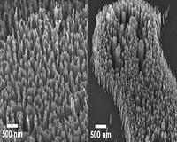 Study Finds More Efficient Means Of Creating, Arranging Carbon Nanofibers
Raleigh NC (SPX) Mar 28, 2011 Carbon nanofibers hold promise for technologies ranging from medical imaging devices to precise scientific measurement tools, but the time and expense associated with uniformly creating nanofibers of the correct size has been an obstacle - until now. A new study from North Carolina State University demonstrates an improved method for creating carbon nanofibers of specific sizes, as well as expla ... read more |
|
| The content herein, unless otherwise known to be public domain, are Copyright 1995-2010 - SpaceDaily. AFP and UPI Wire Stories are copyright Agence France-Presse and United Press International. ESA Portal Reports are copyright European Space Agency. All NASA sourced material is public domain. Additional copyrights may apply in whole or part to other bona fide parties. Advertising does not imply endorsement,agreement or approval of any opinions, statements or information provided by SpaceDaily on any Web page published or hosted by SpaceDaily. Privacy Statement |


 del.icio.us
 Digg
Digg Reddit
 YahooMyWeb
 Google