| . |  |
. |
|
|
. |
by Staff Writers Duisburg, Germany (SPX) Jun 28, 2011
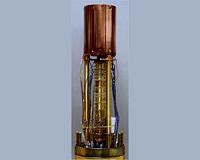
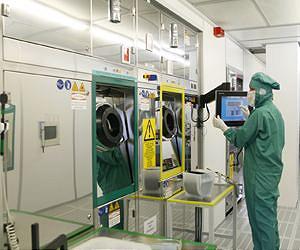
They see more than the naked eye and could make traffic safer: miniaturized thermal imaging sensors. But they are difficult to manufacture on a commercial scale. Researchers have now developed a new system. On it, special micro-electromechanical systems can be produced - with the correct etching technique. A winding country road. It is dark, and a thick ground fog has settled in. The driver of a car cautiously enters the next curve, when suddenly a caution lamp flashes - a fallen motorcycle rider lies on the street. Thanks to the intelligent assistant, the driver has been warned and is able to brake in time. Infrared cameras see more than the naked eye and could make traffic safer. Indeed, thermal imaging cameras are already used in certain applications - in the construction industry and the military, for example. Such infrared cameras, however, are hardly available in the mobile area, for example in automotive safety systems. The reason: long-range infrared microsensors are currently difficult to produce commercially. Researchers of the Fraunhofer Institute for Microelectronic Circuits and Systems IMS in Duisburg, Germany, are now offering a solution. On June 22, they will be opening a new facility in which the production of such micro-system technology, or MST for short, is possible. MST involves minute sensors, valves or other mechanical components that are integrated into semiconductor chips. For instance, in airbags they serve as motion sensors, and they are no thicker than a human hair. If MST is to be applied on semiconductors and integrated, one has to master the art of etching - which is where the researchers at IMS come in. To apply MST to a semiconductor, one essentially puts three layers on top of each other. The bottom layer is the substrate, namely the silicon wafer; in the center there is a sacrificial layer that serves as a spacer, and this is topped by the function layer. The sacrificial layer is later etched away, leaving only the desired sensor structure behind. The problem: "Traditional etching methods allow us only to etch vertically into the layers," explains Dr. Marco Russ, project manager at IMS. "However, unsupported structures are decisive for the mechanical functions of many items of MST." In other words: the etching must work not only vertically but evenly in all directions. Experts call this process "isotropic etching." This ensures that the etching substance not only eats vertically to the substrate but also digs itself under the function layer, like a tunnel. What remains is an unsupported structure of the function layer that is only one hundred nanometers thin and connected to the substrate only at certain suspension points. "A conventional technique is etching with liquids", says Russ. However, capillary forces can occur when the etching fluid dries. The result: the filigree membranes are glued to the substrate or are even destroyed. In addition, most etching liquids do not permit the choice of just any combination of materials for the function and sacrificial layers. "We bypass these problems with our new facility," says Russ. The highlight: "We can use two different gases in the processing chambers of the machine instead of fluids." They are highly selective: hydrogen fluoride (HF) has strong etching properties on silicon dioxide but does not affect silicon. The exact reverse is the case with xenon difluoride gas (XeF2). "This way, we can select which material is better suited to be the function layer," says Russ. The new facility could revolutionize MST production, since the process works in a highly precise manner on an industrial scale. And: whether thermal detectors, acceleration sensors and pressure sensors or micro machines - a multitude of MST structures can be produced in this way. Research News June 2011 [ PDF 386KB ]
|
. |
|
| The content herein, unless otherwise known to be public domain, are Copyright 1995-2011 - Space Media Network. AFP and UPI Wire Stories are copyright Agence France-Presse and United Press International. ESA Portal Reports are copyright European Space Agency. All NASA sourced material is public domain. Additional copyrights may apply in whole or part to other bona fide parties. Advertising does not imply endorsement,agreement or approval of any opinions, statements or information provided by Space Media Network on any Web page published or hosted by Space Media Network. Privacy Statement |
 del.icio.us
 Digg
Digg Reddit
 Google